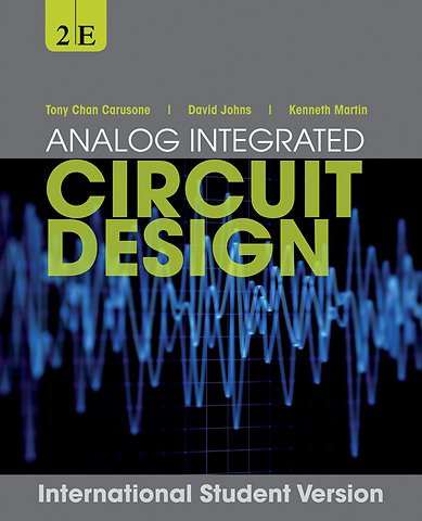
Chan Carusone,
Tony Chan Carusone,
David Johns,
Kenneth Martin
e.a.
Analog Integrated Circuit Design
2e International Student Version WIE
Paperback Engels 2012 2e druk 9781118092330Levertijd ± 8 werkdagen
Gratis verzonden
Samenvatting
The 2
nd Edition of
Analog Integrated Circuit Design focuses on more coverage about several types of circuits that have increased in importance in the past decade. Furthermore, the text is enhanced with material on CMOS IC device modeling, updated processing layout and expanded coverage to reflect technical innovations. CMOS devices and circuits have more influence in this edition as well as a reduced amount of text on BiCMOS and bipolar information. New chapters include topics on frequency response of analog ICs and basic theory of feedback amplifiers.
Specificaties
ISBN13:9781118092330
Taal:Engels
Bindwijze:paperback
Aantal pagina's:832
Uitgever:John Wiley & Sons
Druk:2
Verschijningsdatum:11-5-2012
Hoofdrubriek:IT-management / ICT
Lezersrecensies
Wees de eerste die een lezersrecensie schrijft!
Inhoudsopgave
CHAPTER 1 INTEGRATED–CIRCUIT DEVICES AND MODELLING 1
1.1 Semiconductors and pn Junctions 1
1.1.1 Diodes 2
1.1.2 Reverse–Biased Diodes 4
1.1.3 Graded Junctions 8
1.1.4 Large–Signal Junction Capacitance 10
1.1.5 Forward–Biased Junctions 11
1.1.6 Junction Capacitance of Forward–Biased Diode 12
1.1.7 Small–Signal Model of a Forward–Biased Diode 13
1.1.8 Schottky Diodes 14
1.2 MOS Transistors 15
1.2.1 Symbols for MOS Transistors 16
1.2.2 Basic Operation 17
1.2.3 Large–Signal Modelling 22
1.2.4 Body Effect 25
1.2.5 p–Channel Transistors 26
1.2.6 Low–Frequency Small–Signal Modelling in the Active Region 26
1.2.7 High–Frequency Small–Signal Modelling in the Active Region 32
1.2.8 Small–Signal Modelling in the Triode and Cutoff Regions 35
1.2.9 Analog Figures of Merit and Trade–offs 37
1.3 Device Model Summary 39
1.3.1 Constants 40
1.3.2 Diode Equations 40
1.3.3 MOS Transistor Equations 41
1.4 Advanced MOS Modelling 43
1.4.1 Subthreshold Operation 43
1.4.2 Mobility Degradation 46
1.4.3 Summary of Subthreshold and Mobility Degradation Equations 48
1.4.4 Parasitic Resistances 48
1.4.5 Short–Channel Effects 49
1.4.6 Leakage Currents 50
1.5 SPICE Modelling Parameters 51
1.5.1 Diode Model 51
1.5.2 MOS Transistors 52
1.5.3 Advanced SPICE Models of MOS Transistors 52
1.6 Passive Devices 55
1.6.1 Resistors 55
1.6.2 Capacitors 59
1.7 Appendix 61
1.7.1 Diode Exponential Relationship 61
1.7.2 Diode–Diffusion Capacitance 63
1.7.3 MOS Threshold Voltage and the Body Effect 65
1.7.4 MOS Triode Relationship 67
1.8 Key Points 69
1.9 References 70
1.10 Problems 70
CHAPTER 2 PROCESSING AND LAYOUT 73
2.1 CMOS Processing 73
2.1.1 The Silicon Wafer 73
2.1.2 Photolithography and Well Definition 74
2.1.3 Diffusion and Ion Implantation 76
2.1.4 Chemical Vapor Deposition and Defining the Active Regions 78
2.1.5 Transistor Isolation 78
2.1.6 Gate–Oxide and Threshold–Voltage Adjustments 81
2.1.7 Polysilicon Gate Formation 82
2.1.8 Implanting the Junctions, Depositing SiO2, and Opening Contact Holes 82
2.1.9 Annealing, Depositing and Patterning Metal, and Overglass Deposition 84
2.1.10 Additional Processing Steps 84
2.2 CMOS Layout and Design Rules 86
2.2.1 Spacing Rules 86
2.2.2 Planarity and Fill Requirements 94
2.2.3 Antenna Rules 94
2.2.4 Latch–Up 95
2.3 Variability and Mismatch 96
2.3.1 Systematic Variations Including Proximity Effects 96
2.3.2 Process Variations 98
2.3.3 Random Variations and Mismatch 99
2.4 Analog Layout Considerations 103
2.4.1 Transistor Layouts 103
2.4.2 Capacitor Matching 104
2.4.3 Resistor Layout 107
2.4.4 Noise Considerations 109
2.5 Key Points 112
2.6 References 113
2.7 Problems 114
CHAPTER 3 BASIC CURRENT MIRRORS AND SINGLE–STAGE AMPLIFIERS 117
3.1 Simple CMOS Current Mirror 118
3.2 Common–Source Amplifier 120
3.3 Source–Follower or Common–Drain Amplifier 122
3.4 Common–Gate Amplifier 124
3.5 Source–Degenerated Current Mirrors 127
3.6 Cascode Current Mirrors 129
3.7 Cascode Gain Stage 131
3.8 MOS Differential Pair and Gain Stage 135
3.9 Key Points 138
3.10 References 139
3.11 Problems 139
CHAPTER 4 FREQUENCY RESPONSE OF ELECTRONIC CIRCUITS 144
4.1 Frequency Response of Linear Systems 144
4.1.1 Magnitude and Phase Response 145
4.1.2 First–Order Circuits 147
4.1.3 Second–Order Low–Pass Transfer Functions with Real Poles 154
4.1.4 Bode Plots 157
4.1.5 Second–Order Low–Pass Transfer Functions with Complex Poles 163
4.2 Frequency Response of Elementary Transistor Circuits 164
4.2.1 High–Frequency MOS Small–Signal Model 164
4.2.2 Common–Source Amplifier 166
4.2.3 Miller Theorem and Miller Effect 169
4.2.4 Zero–Value Time–Constant Analysis 173
4.2.5 Common–Source Design Examples 176
4.2.6 Common–Gate Amplifier 179
4.3 Cascode Gain Stage 181
4.4 Source–Follower Amplifier 187
4.5 Differential Pair 193
4.5.1 High–Frequency T Model 193
4.5.2 Symmetric Differential Amplifier 194
4.5.3 Single–Ended Differential Amplifier 195
4.5.4 Differential Pair with Active Load 196
4.6 Key Points 197
4.7 References 198
4.8 Problems 198
CHAPTER 5 FEEDBACK AMPLIFIERS 204
5.1 Ideal Model of Negative Feedback 204
5.1.1 Basic Definitions 204
5.1.2 Gain Sensitivity 205
5.1.3 Bandwidth 206
5.1.4 Linearity 207
5.1.5 Summary 207
5.2 Dynamic Response of Feedback Amplifiers 208
5.2.1 Stability Criteria 209
5.2.2 Phase Margin 211
5.3 First– and Second–Order Feedback Systems 213
5.3.1 First–Order Feedback Systems 213
5.3.2 Second–Order Feedback Systems 217
5.3.3 Higher–Order Feedback Systems 220
5.4 Common Feedback Amplifiers 221
5.4.1 Obtaining the Loop Gain, L(s) 222
5.4.2 Noninverting Amplifier 226
5.4.3 Transimpedance (Inverting) Amplifiers 231
5.5 Summary of Key Points 235
5.6 References 236
5.7 Problems 236
CHAPTER 6 BASIC OPAMP DESIGN AND COMPENSATION 242
6.1 Two–Stage CMOS Opamp 242
6.1.1 Opamp Gain 243
6.1.2 Frequency Response 245
6.1.3 Slew Rate 249
6.1.4 n–Channel or p–Channel Input Stage 252
6.1.5 Systematic Offset Voltage 253
6.2 Opamp Compensation 254
6.2.1 Dominant–Pole Compensation and Lead Compensation 255
6.2.2 Compensating the Two–Stage Opamp 256
6.2.3 Making Compensation Independent of Process and Temperature 260
6.3 Advanced Current Mirrors 262
6.3.1 Wide–Swing Current Mirrors 262
6.3.2 Enhanced Output–Impedance Current Mirrors and Gain Boosting 263
6.3.3 Wide–Swing Current Mirror with Enhanced Output Impedance 266
6.3.4 Current–Mirror Symbol 267
6.4 Folded–Cascode Opamp 268
6.4.1 Small–Signal Analysis 270
6.4.2 Slew Rate 272
6.5 Current Mirror Opamp 275
6.6 Linear Settling Time Revisited 279
6.7 Fully Differential Opamps 281
6.7.1 Fully Differential Folded–Cascode Opamp 283
6.7.2 Alternative Fully Differential Opamps 284
6.7.3 Low Supply Voltage Opamps 286
6.8 Common–Mode Feedback Circuits 288
6.9 Summary of Key Points 292
6.10 References 293
6.11 Problems 294
CHAPTER 7 BIASING, REFERENCES, AND REGULATORS 302
7.1 Analog Integrated Circuit Biasing 302
7.1.1 Bias Circuits 303
7.1.2 Reference Circuits 305
7.1.3 Regulator Circuits 306
7.2 Establishing Constant Transconductance 307
7.2.1 Basic Constant–Transconductance Circuit 307
7.2.2 Improved Constant–Transconductance Circuits 309
7.3 Establishing Constant Voltages and Currents 310
7.3.1 Bandgap Voltage Reference Basics 310
7.3.2 Circuits for Bandgap References 314
7.3.3 Low–Voltage Bandgap Reference 319
7.3.4 Current Reference 320
7.4 Voltage Regulation 321
7.4.1 Regulator Specifications 321
7.4.2 Feedback Analysis 322
7.4.3 Low Dropout Regulators 324
7.5 Summary of Key Points 327
7.6 References 327
7.7 Problems 328
CHAPTER 8 BIPOLAR DEVICES AND CIRCUITS 331
8.1 Bipolar–Junction Transistors 331
8.1.1 Basic Operation 331
8.1.2 Analog Figures of Merit 341
8.2 Bipolar Device Model Summary 344
8.3 SPICE Modeling 345
8.4 Bipolar and BICMOS Processing 346
8.4.1 Bipolar Processing 346
8.4.2 Modern SiGe BiCMOS HBT Processing 347
8.4.3 Mismatch in Bipolar Devices 348
8.5 Bipolar Current Mirrors and Gain Stages 349
8.5.1 Current Mirrors 349
8.5.2 Emitter Follower 350
8.5.3 Bipolar Differential Pair 353
8.6 Appendix 356
8.6.1 Bipolar Transistor Exponential Relationship 356
8.6.2 Base Charge Storage of an Active BJT 359
8.7 Summary of Key Points 359
8.8 References 360
8.9 Problems 360
CHAPTER 9 NOISE AND LINEARITY ANALYSIS AND MODELLING 363
9.1 Time–Domain Analysis 363
9.1.1 Root Mean Square (rms) Value 364
9.1.2 SNR 365
9.1.3 Units of dBm 365
9.1.4 Noise Summation 366
9.2 Frequency–Domain Analysis 367
9.2.1 Noise Spectral Density 367
9.2.2 White Noise 369
9.2.3 1/f, or Flicker, Noise 370
9.2.4 Filtered Noise 371
9.2.5 Noise Bandwidth 373
9.2.6 Piecewise Integration of Noise 375
9.2.7 1/f Noise Tangent Principle 377
9.3 Noise Models for Circuit Elements 377
9.3.1 Resistors 378
9.3.2 Diodes 378
9.3.3 Bipolar Transistors 380
9.3.4 MOSFETS 380
9.3.5 Opamps 382
9.3.6 Capacitors and Inductors 382
9.3.7 Sampled Signal Noise 384
9.3.8 Input–Referred Noise 384
9.4 Noise Analysis Examples 387
9.4.1 Opamp Example 387
9.4.2 Bipolar Common–Emitter Example 390
9.4.3 CMOS Differential Pair Example 392
9.4.4 Fiber–Optic Transimpedance Amplifier Example 395
9.5 Dynamic Range Performance 397
9.5.1 Total Harmonic Distortion (THD) 398
9.5.2 Third–Order Intercept Point (IP3) 400
9.5.3 Spurious–Free Dynamic Range (SFDR) 402
9.5.4 Signal–to–Noise and Distortion Ratio (SNDR) 404
9.6 Key Points 405
9.7 References 406
9.8 Problems 406
CHAPTER 10 COMPARATORS 413
10.1 Comparator Specifications 413
10.1.1 Input Offset and Noise 413
10.1.2 Hysteresis 414
10.2 Using an Opamp for a Comparator 415
10.2.1 Input–Offset Voltage Errors 417
10.3 Charge–Injection Errors 418
10.3.1 Making Charge–Injection Signal Independent 421
10.3.2 Minimizing Errors Due to Charge–Injection 421
10.3.3 Speed of Multi–Stage Comparators 424
10.4 Latched Comparators 426
10.4.1 Latch–Mode Time Constant 428
10.4.2 Latch Offset 430
10.5 Examples of CMOS and BiCMOS Comparators 432
10.5.1 Input–Transistor Charge Trapping 435
10.6 Examples of Bipolar Comparators 437
10.7 Key Points 439
10.8 References 440
10.9 Problems 441
CHAPTER 11 SAMPLE–AND–HOLD AND TRANSLINEAR CIRCUITS 444
11.1 Performance of Sample–and–Hold Circuits 444
11.1.1 Testing Sample–and–Holds 445
11.2 MOS Sample–and–Hold Basics 446
11.3 Examples of CMOS S/H Circuits 452
11.4 Bipolar and BiCMOS Sample–and–Holds 456
11.5 Translinear Gain Cell 460
11.6 Translinear Multiplier 462
11.7 Key Points 464
11.8 References 465
11.9 Problems 466
CHAPTER 12 CONTINUOUS–TIME FILTERS 469
12.1 Introduction to Continuous–Time Filters 469
12.1.1 First–Order Filters 470
12.1.2 Second–Order Filters 470
12.2 Introduction to Gm–C Filters 471
12.2.1 Integrators and Summers 472
12.2.2 Fully Differential Integrators 473
12.2.3 First–Order Filter 475
12.2.4 Biquad Filter 477
12.3 Transconductors Using Fixed Resistors 478
12.4 CMOS Transconductors Using Triode Transistors 483
12.4.1 Transconductors Using a Fixed–Bias Triode Transistor 484
12.4.2 Transconductors Using Varying Bias–Triode Transistors 486
12.4.3 Transconductors Using Constant Drain–Source Voltages 490
12.5 CMOS Transconductors Using Active Transistors 492
12.5.1 CMOS Pair 493
12.5.2 Constant Sum of Gate–Source Voltages 494
12.5.3 Source–Connected Differential Pair 495
12.5.4 Inverter–Based 495
12.5.5 Differential–Pair with Floating Voltage Sources 496
12.5.6 Bias–Offset Cross–Coupled Differential Pairs 499
12.6 Bipolar Transconductors 499
12.6.1 Gain–Cell Transconductors 500
12.6.2 Transconductors Using Multiple Differential Pairs 502
12.7 BiCMOS Transconductors 506
12.7.1 Tunable MOS in Triode 506
12.7.2 Fixed–Resistor Transconductor with a Translinear Multiplier 507
12.7.3 Fixed Active MOS Transconductor with a Translinear Multiplier 508
12.8 Active RC and MOSFET–C Filters 509
12.8.1 Active RC Filters 510
12.8.2 MOSFET–C Two–Transistor Integrators 512
12.8.3 Four–Transistor Integrators 515
12.8.4 R–MOSFET–C Filters 516
12.9 Tuning Circuitry 517
12.9.1 Tuning Overview 517
12.9.2 Constant Transconductance 519
12.9.3 Frequency Tuning 520
12.9.4 Q–Factor Tuning 522
12.9.5 Tuning Methods Based on Adaptive Filtering 523
12.10 Introduction to Complex Filters 525
12.10.1 Complex Signal Processing 525
12.10.2 Complex Operations 526
12.10.3 Complex Filters 527
12.10.4 Frequency–Translated Analog Filters 528
12.11 Key Points 531
12.12 References 532
12.13 Problems 534
CHAPTER 13 DISCRETE–TIME SIGNALS 537
13.1 Overview of Some Signal Spectra 537
13.2 Laplace Transforms of Discrete–Time Signals 537
13.2.1 Spectra of Discrete–Time Signals 540
13.3 z–Transform 541
13.4 Downsampling and Upsampling 543
13.5 Discrete–Time Filters 545
13.5.1 Frequency Response of Discrete–Time Filters 545
13.5.2 Stability of Discrete–Time Filters 548
13.5.3 IIR and FIR Filters 550
13.5.4 Bilinear Transform 550
13.6 Sample–and–Hold Response 552
13.7 Key Points 554
13.8 References 555
13.9 Problems 555
CHAPTER 14 SWITCHED–CAPACITOR CIRCUITS 557
14.1 Basic Building Blocks 557
14.1.1 Opamps 557
14.1.2 Capacitors 558
14.1.3 Switches 558
14.1.4 Nonoverlapping Clocks 559
14.2 Basic Operation and Analysis 560
14.2.1 Resistor Equivalence of a Switched Capacitor 560
14.2.2 Parasitic–Sensitive Integrator 563
14.2.3 Parasitic–Insensitive Integrators 565
14.2.4 Signal–Flow–Graph Analysis 569
14.3 Noise in Switched–Capacitor Circuits 570
14.4 First–Order Filters 572
14.4.1 Switch Sharing 575
14.4.2 Fully Differential Filters 575
14.5 Biquad Filters 577
14.5.1 Low–Q Biquad Filter 577
14.5.2 High–Q Biquad Filter 581
14.6 Charge Injection 585
14.7 Switched–Capacitor Gain Circuits 588
14.7.1 Parallel Resistor–Capacitor Circuit 588
14.7.2 Resettable Gain Circuit 588
14.7.3 Capacitive–Reset Gain Circuit 591
14.8 Correlated Double–Sampling Techniques 593
14.9 Other Switched–Capacitor Circuits 594
14.9.1 Amplitude Modulator 594
14.9.2 Full–Wave Rectifier 595
14.9.3 Peak Detectors 596
14.9.4 Voltage–Controlled Oscillator 596
14.9.5 Sinusoidal Oscillator 598
14.10 Key Points 600
14.11 References 601
14.12 Problems 602
CHAPTER 15 DATA CONVERTER FUNDAMENTALS 606
15.1 Ideal D/A Converter 606
15.2 Ideal A/D Converter 608
15.3 Quantization Noise 609
15.3.1 Deterministic Approach 609
15.3.2 Stochastic Approach 610
15.4 Signed Codes 612
15.5 Performance Limitations 614
15.5.1 Resolution 614
15.5.2 Offset and Gain Error 615
15.5.3 Accuracy and Linearity 615
15.6 Key Points 620
15.7 References 620
15.8 Problems 620
CHAPTER 16 NYQUIST–RATE D/A CONVERTERS 623
16.1 Decoder–Based Converters 623
16.1.1 Resistor–String Converters 623
16.1.2 Folded Resistor–String Converters 625
16.1.3 Multiple Resistor–String Converters 626
16.1.4 Signed Outputs 628
16.2 Binary–Scaled Converters 629
16.2.1 Binary–Weighted Resistor Converters 629
16.2.2 Reduced–Resistance–Ratio Ladders 630
16.2.3 R–2R–Based Converters 631
16.2.4 Charge–Redistribution Switched–Capacitor Converters 632
16.2.5 Current–Mode Converters 633
16.2.6 Glitches 633
16.3 Thermometer–Code Converters 634
16.3.1 Thermometer–Code Current–Mode D/A Converters 636
16.3.2 Single–Supply Positive–Output Converters 637
16.3.3 Dynamically Matched Current Sources 638
16.4 Hybrid Converters 640
16.4.1 Resistor–Capacitor Hybrid Converters 640
16.4.2 Segmented Converters 640
16.5 Key Points 642
16.6 References 643
16.7 Problems 643
CHAPTER 17 NYQUIST–RATE A/D CONVERTERS 646
17.1 Integrating Converters 646
17.2 Successive–Approximation Converters 650
17.2.1 D/A–Based Successive Approximation 652
17.2.2 Charge–Redistribution A/D 653
17.2.3 Resistor–Capacitor Hybrid 658
17.2.4 Speed Estimate for Charge–Redistribution Converters 659
17.2.5 Error Correction in Successive–Approximation Converters 660
17.2.6 Multi–Bit Successive–Approximation 662
17.3 Algorithmic (or Cyclic) A/D Converter 662
17.3.1 Ratio–Independent Algorithmic Converter 663
17.4 Pipelined A/D Converters 667
17.4.1 One–Bit–Per–Stage Pipelined Converter 667
17.4.2 1.5 Bit Per Stage Pipelined Converter 670
17.4.3 Pipelined Converter Circuits 673
17.4.4 Generalized k–Bit–Per–Stage Pipelined Converters 673
17.5 Flash Converters 674
17.5.1 Issues in Designing Flash A/D Converters 675
17.6 Two–Step A/D Converters 678
17.6.1 Two–Step Converter with Digital Error Correction 679
17.7 Interpolating A/D Converters 681
17.8 Folding A/D Converters 684
17.9 Time–Interleaved A/D Converters 687
17.10 Key Points 690
17.11 References 691
17.12 Problems 692
CHAPTER 18 OVERSAMPLING CONVERTERS 696
18.1 Oversampling without Noise Shaping 696
18.1.1 Quantization Noise Modelling 697
18.1.2 White Noise Assumption 697
18.1.3 Oversampling Advantage 698
18.1.4 The Advantage of 1–Bit D/A Converters 700
18.2 Oversampling with Noise Shaping 701
18.2.1 Noise–Shaped Delta–Sigma Modulator 702
18.2.2 First–Order Noise Shaping 703
18.2.3 Switched–Capacitor Realization of a First–Order A/D Converter 705
18.2.4 Second–Order Noise Shaping 705
18.2.5 Noise Transfer–Function Curves 707
18.2.6 Quantization Noise Power of 1–Bit Modulators 708
18.2.7 Error–Feedback Structure 708
18.3 System Architectures 710
18.3.1 System Architecture of Delta–Sigma A/D Converters 710
18.3.2 System Architecture of Delta–Sigma D/A Converters 712
18.4 Digital Decimation Filters 713
18.4.1 Multi–Stage 714
18.4.2 Single Stage 716
18.5 Higher–Order Modulators 717
18.5.1 Interpolative Architecture 717
18.5.2 Multi–Stage Noise Shaping (MASH) Architecture 718
18.6 Bandpass Oversampling Converters 720
18.7 Practical Considerations 721
18.7.1 Stability 721
18.7.2 Linearity of Two–Level Converters 722
18.7.3 Idle Tones 724
18.7.4 Dithering 725
18.7.5 Opamp Gain 725
18.8 Multi–Bit Oversampling Converters 726
18.8.1 Dynamic Element Matching 726
18.8.2 Dynamically Matched Current Source D/A Converters 727
18.8.3 Digital Calibration A/D Converter 727
18.8.4 A/D with Both Multi–Bit and Single–Bit Feedback 728
18.9 Third–Order A/D Design Example 729
18.10 Key Points 731
18.11 References 733
18.12 Problems 734
CHAPTER 19 PHASE–LOCKED LOOPS 737
19.1 Basic Phase–Locked Loop Architecture 737
19.1.1 Voltage–Controlled Oscillator 738
19.1.2 Divider 739
19.1.3 Phase Detector 740
19.1.4 Loop Filer 745
19.1.5 The PLL in Lock 746
19.2 Linearized Small–Signal Analysis 747
19.2.1 Second–Order PLL Model 748
19.2.2 Limitations of the Second–Order Small–Signal Model 750
19.2.3 PLL Design Example 752
19.3 Jitter and Phase Noise 754
19.3.1 Period Jitter 758
19.3.2 P–Cycle Jitter 758
19.3.3 Adjacent Period Jitter 759
19.3.4 Other Spectral Representations of Jitter 760
19.3.5 Probability Density Function of Jitter 761
19.4 Electronic Oscillators 763
19.4.1 Ring Oscillators 764
19.4.2 LC Oscillators 768
19.4.3 Phase Noise of Oscillators 770
19.5 Jitter and Phase Noise in PLLS 774
19.5.1 Input Phase Noise and Divider Phase Noise 775
19.5.2 VCO Phase Noise 775
19.5.3 Loop Filter Noise 776
19.6 Key Points 779
19.7 References 779
19.8 Problems 780
INDEX 783
Afgekapt op 60 regels
Rubrieken
- advisering
- algemeen management
- coaching en trainen
- communicatie en media
- economie
- financieel management
- inkoop en logistiek
- internet en social media
- it-management / ict
- juridisch
- leiderschap
- marketing
- mens en maatschappij
- non-profit
- ondernemen
- organisatiekunde
- personal finance
- personeelsmanagement
- persoonlijke effectiviteit
- projectmanagement
- psychologie
- reclame en verkoop
- strategisch management
- verandermanagement
- werk en loopbaan