,

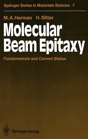
Molecular Beam Epitaxy

Fundamentals and Current Status

Paperback Engels 2012 9783642971006
€ 60,99
Levertijd ongeveer 9 werkdagen
Gratis verzonden

Samenvatting

Since a molecular-beam apparatus was first successfully used by Cho and Arthur in the late 1960s to crystallize and investigate GaAs epilayers, high vacuum epitaxial growth techniques using particle beams have developed rapidly. This development accelerated when different semiconductor devices with quantum­ well structures were invented in the 1970s. The important implementation of these structures in devices like quantum-well lasers, high electron mobility tran­ sistors or superlattice avalanche photodiodes gave added impetus to research work and to increasing production aims. Coincident with this development, orig­ inal research papers and reviews devoted to problems concerning these growth techniques have also rapidly grown in number, and in addition they have become very disversified. At present several hundred original papers on this subject ap­ pear in the literature each year. However, in contrast to this there is a lack of comprehensive monographs comprising the whole variety of problems related to epitaxial growth of semiconductor films from atomic and molecular beams. This book, which presents a review of the state of the art of molecular beam epitaxy (MBE), as applied to the growth of semiconductor films and multilayer structures, may serve the reader as a convenient general guide to the topics related to this crystallization technique.

Specificaties

ISBN13:9783642971006
Taal:Engels
Bindwijze:paperback
Aantal pagina's:382
Uitgever:Springer Berlin Heidelberg

Lezersrecensies

Wees de eerste die een lezersrecensie schrijft!

Inhoudsopgave

I Background Information.- 1. Introduction.- 1.1 Thin Film Growth from Beams in a High Vacuum Environment.- 1.1.1 Vacuum Conditions for MBE.- 1.1.2 Basic Physical Processes in the MBE Vacuum Chamber.- 1.2 Evolution of the MBE Technique.- 1.2.1 The Early Stages of MBE.- 1.2.2 MBE in the 1980s.- 1.3 Modifications of the MBE Technique.- 1.3.1 Gas Source MBE.- 1.3.2 Phase-Locked Epitaxy.- 1.3.3 Atomic Layer Epitaxy.- 1.3.4 FIBI-MBE Processing Technology.- 1.3.5 A Classification Scheme for the MBE Techniques.- II Technological Equipment.- 2. Sources of Atomic and Molecular Beams.- 2.1 The Effusion Process and the Ideal Effusion Cell.- 2.1.1 Langmuir and Knudsen Modes of Evaporation.- 2.1.2 The Cosine Law of Effusion.- 2.2 Effusion from Real Effusion Cells.- 2.2.1 The Near-Ideal Cylindrical Effusion Cell.- 2.2.2 The Cylindrical Channel Effusion Cell.- 2.2.3 Hot-Wall Beam Cylindrical Source.- 2.2.4 The Conical Effusion Cell.- 2.3 Effusion Cells Used in CPS MBE Systems.- 2.3.1 Conventional Effusion Cells.- 2.3.2 Dissociation (Cracker) Effusion Cells.- 2.3.3 Electron Beam and Laser Radiation Heated Sources.- 2.4 Beam Sources Used in GS MBE Systems.- 2.4.1 Arsine and Phosphine Gas Source Crackers.- 2.4.2 Gas Sources Used in MO MBE.- 3. High Vacuum Growth and Processing Systems.- 3.1 Building Blocks of Modular MBE Systems.- 3.1.1 The Cassette Entry Stage.- 3.1.2 The Interstage Substrate Transfer System.- 3.1.3 The Preparation and Analysis Stages.- 3.1.4 The MBE Deposition Chamber.- 3.1.5 Beam Sources.- 3.1.6 Monitoring and Analytical Facilities.- 3.2 Multiple-Growth and Multiple-Process Facilities in MBE Systems.- 3.2.1 The Hot-Wall Beam Epitaxy Growth System.- 3.2.2 Focused Ion Beam Technology.- III Characterization Methods.- 4. In-Growth Characterization Techniques.- 4.1 RHEED.- 4.1.1 Fundamentals of Electron Diffraction.- 4.1.2 Origin of RHEED Features.- 4.1.3 RHEED Data from Reconstructed Semiconductor Surfaces.- 4.1.4 RHEED Rocking Curves.- 4.1.5 RHEED Intensity Oscillations.- 4.2 Ellipsometry.- 4.2.1 Fundamentals of Ellipsometry.- 4.2.2 Ellipsometric Systems Used for In-Growth Analysis in MBE.- 5. Postgrowth Characterization Methods.- 5.1 Survey of Postgrowth Characterization Methods.- 5.2 Auger Electron Spectroscopy.- 5.2.1 Chemical Composition of Solid Surfaces.- 5.2.2 Sputter Depth Profiling.- 5.3 X-Ray Diffraction.- 5.3.1 Diffraction Under Nonideal Conditions.- 5.3.2 High Resolution X-Ray Diffraction.- 5.3.3 X-Ray Diffraction at Multilayers and Superlattices.- 5.4 Photoluminescence.- 5.4.1 Photoluminescence in Binary Compounds.- 5.4.2 Photoluminescence in Ternary and Quaternary Compounds.- 5.4.3 Photoluminescence of Quantum Well Structures and Superlattices.- 5.5 Electrical Characterization.- 5.5.1 Determination of Carrier Concentration and Mobility.- 5.5.2 Deep Level Transient Spectroscopy.- 5.6 Sophisticated Characterization Methods.- 5.6.1 Transmission Electron Microscopy.- 5.6.2 Rutherford Backscattering and Channeling.- IV MBE Growth Processes.- 6. Fundamentals of the MBE Growth Process.- 6.1 General View of the MBE Growth Process.- 6.1.1 Equilibrium States in MBE.- 6.1.2 The Transition Layer Concept.- 6.2 Relations Between Substrate and Epilayer.- 6.2.1 Critical Thickness for the Formation of Misfit Dislocations.- 6.2.2 Role of the Crystallographic Orientation of the Substrate.- 6.2.3 Role of the Substrate Surface Reconstruction.- 6.3 The Near-Surface Transition Layer.- 6.3.1 Physical and Chemical Adsorption.- 6.3.2 Spatial Arrangement of the Near-Surface Transition Layer.- 6.4 Growth Interruption and Pulsed Beam Deposition.- 6.4.1 Recovery Effect During Growth Interruption.- 6.4.2 Growth of Superlattice Structures by Phase-Locked Epitaxy.- 6.4.3 UHV Atomic Layer Epitaxy.- 6.4.4 Migration Enhanced Epitaxy.- 6.4.5 Molecular Layer Epitaxy.- 6.5 Doping During MBE Processes.- 6.5.1 Unintentional Doping.- 6.5.2 Thermodynamics of Doping by Co-deposition.- 6.5.3 Delta-Function-Like Doping Profiles.- 6.5.4 In-Growth Doping with Ionized Beams.- 7. Material-Related Growth Characteristics in MBE.- 7.1 Si and IV-IV Heterostructures.- 7.1.1 Si Substrate Preparation Procedures.- 7.1.2 Homoepitaxy of Si Films.- 7.1.3 Heteroepitaxy of Ge and Sn on Si Substrates.- 7.1.4 GexSi1-x/Si Heterostructures and Superlattices.- 7.1.5 Devices Grown by Si MBE.- 7.2 GaAs- and As-Containing Compounds.- 7.2.1 Preparation of the GaAs(100) Substrate Surface.- 7.2.2 Growth of GaAs on GaAs(100) Substrates.- 7.2.3 Growth of AlxGa1-xAs/GaAs Heterostructures.- 7.2.4 Growth of GaAs on Si Substrates.- 7.2.5 Device Structures Grown by GaAs MBE.- 7.3 Narrow-Gap II-VI Compounds Containing Hg.- 7.3.1 Substrates for MBE of Hg Compounds.- 7.3.2 Hg-Compound Heterostructures Grown by MBE.- 7.3.3 Device Structures.- V Conclusion.- 8. Outlook.- 8.1 Miscellaneous Material Systems Grown by MBE.- 8.2 MBE-Related Growth Techniques.- 8.3 Development Trends of the MBE Technique.- References.

Managementboek Top 100

€ 60,99
Levertijd ongeveer 9 werkdagen
Gratis verzonden

Rubrieken

    Personen

      Trefwoorden

        Molecular Beam Epitaxy