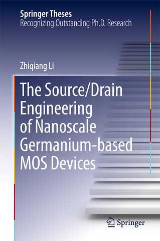
The Source/Drain Engineering of Nanoscale Germanium-based MOS Devices
Gebonden Engels 2016 9783662496817Samenvatting
This book mainly focuses on reducing the high parasitic resistance in the source/drain of germanium nMOSFET. With adopting of the Implantation After Germanide (IAG) technique, P and Sb co-implantation technique and Multiple Implantation and Multiple Annealing (MIMA) technique, the electron Schottky barrier height of NiGe/Ge contact is modulated to 0.1eV, the thermal stability of NiGe is improved to 600℃ and the contact resistivity of metal/n-Ge contact is drastically reduced to 3.8×10⁻⁷Ω•cm2, respectively. Besides, a reduced source/drain parasitic resistance is demonstrated in the fabricated Ge nMOSFET. Readers will find useful information about the source/drain engineering technique for high-performance CMOS devices at future technology node.
Specificaties
Lezersrecensies
Inhoudsopgave
Rubrieken
- advisering
- algemeen management
- coaching en trainen
- communicatie en media
- economie
- financieel management
- inkoop en logistiek
- internet en social media
- it-management / ict
- juridisch
- leiderschap
- marketing
- mens en maatschappij
- non-profit
- ondernemen
- organisatiekunde
- personal finance
- personeelsmanagement
- persoonlijke effectiviteit
- projectmanagement
- psychologie
- reclame en verkoop
- strategisch management
- verandermanagement
- werk en loopbaan